Acoustical Society of America
ASA/EAA/DAGA '99 Meeting
Lay Language Papers
Silicon Microphones: An Overview
Marc Fischer fis@uet.tu-darmstadt.de
Gerhard M. Sessler
Fachgebiet Elektroakustik
Merckstrasse 25
64283 Darmstadt
Germany
Silicon Sensors : An Overview, Popular version of paper 2aEA
Presented Tuesday morning, March 16, 1999
ASA/EAA/DAGA '99 Meeting, Berlin, Germany
Introduction
Over the past few years the field of silicon micromachining has become a well established technology. This development was advanced by the prospect of being able to produce new types of sensors and to fabricate them at low cost.
This paper will present a brief overview of the standard micromachining techniques and of the different silicon microphone principles.
Sketches in this paper are not according to scale !
Why micromachining ?
A main reason for using micromachining is cost reduction.
By having a large number of sensors on a chip, one can process them simultaniously (batch processing). Micromachining makes it possible to control layer thicknesses and lateral dimensions precisely within the sub micron range. High absolute precision and reproducibility is the result. Another advantage which lowers the price of the components is the possibility of integrating passive and active electronic devices on the
same chip together with the sensor.
By using silicon micromachining, one is able to design new types of sensors utilizing the special mechanical and electrical properties of silicon.
In addition, micromachined microphones are less vibration-sensitive than conventional ones.
Micromachining
The design of micromechanical sensors is strongly influenced by the technology offered by micromachining.
This means that one is restricted in the choice of geometry and design of the microphones.
This is complicated by the desire to use only standard techniques (e.g. as used in CMOS processes) to keep the production costs low and to treat wafers only in a way that electrical components are not influenced by the treatment. This is necessary to permit integration of electronics with the sensor.
There are three main procedures to build up micromechanical components : removing material, depositing material and patterning material.
Characteristic for the depositing (e.g. evaporation) and the removing procedures (e.g. etching) is that they normally affect the whole surface of the wafer. This makes it necessary to protect those areas which don't have to be processed. This is done by masking.
The patterning for defining lateral structures is performed by a lithography process which is similar to those processes used to fabricate printed circuit boards.
Typical dimensions for the thickness of vertical layers are in the range of 10 nm .. 10 m and for lateral dimensions in the range of 1m .. 1cm.
Fabrication of a Membrane chip
In the following, the fabrication of a membrane chip is briefly explained to give an idea about micromachining. The fabrication of a membrane starts with depositing the membrane material on the front side of the wafer. This is a critical process step, because the properties of the deposited layer influence the mechanical characteristics and therefore the acoustical behaviour strongly. The internal stress , for example, is an important factor for the value of the resonance frequency.
Step two is to deposit a masking layer on the backside of the wafer. This has to be resistant against the etch solution with which the grooves are etched.
Before etching the wafer, this masking layer has to be patterned. This is done by a lithography process followed by an etch step which removes those areas exposed to the etch solution. Figure 1 shows the wafer after stripping the photoresist.
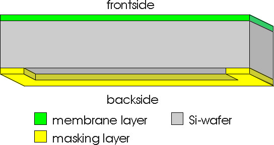 Fig. 1
By using an anisotropic (direction depending) etch solution one gets grooves with the characteristic v-shape (fig 2). Since the deposited membrane layer consists of an etch-resistant material, it survives the etch process and forms the membrane.
Typical dimensions are : wafer thickness : 500 m, membrane thickness : usually in submicron range, lateral membrane size in the range of 1mm by 1mm.
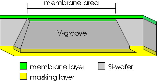 Fig. 2
Capacitive Microphones
Conventional capacitive microphones, in particular electret microphones, are most frequently used because of their good acoustical properties and their low price.
Early attempts were made to realize this principle with the methods of micromechanics.
Figure 3 shows a typical two chip design. The membrane is realized on one chip and the backplate on the other. The spacer is realized by a layer deposited on the backplate chip.
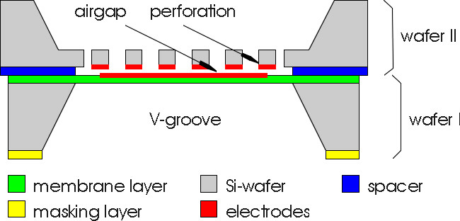 Fig. 3
Figure 4 shows a single chip design. The sacrificial layer and the backplate layer is deposited on top of the
membrane chip. The structure arises by removing (etching) the sacrificial layer between backplate and
membrane.
Both designs were made using bulk micromachining. This means that the wafer has to be processed from the front and the back. The single chip microphone has the advantage that only one type of wafer has to be processed and that the critical step of glueing two wafers together is unnecessary. The disadvantage is the more complex production compared with a two chip design. Two chip designs offer easier ways to optimize each part (membrane and backplate)
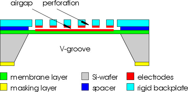 Fig. 4
Piezoresistive Microphones
Piezoresistive microphones are one chip designs (fig. 5). They are utilizing materials which change their electrical resistivity with the mechanical stress in the layer. Main part is the membrane covered by piezoresistive resistors. Deflection caused by a soundwave results in mechanical stress in the active layers. The change in resistivity is proportional to the stress and indirectly to the deflection. One can use polycrystalline silicon or monocrystalline silicon as the piezoresistive layer.
Normally, four resistors are combined in a Wheatstone bridge to increase the sensitivity.
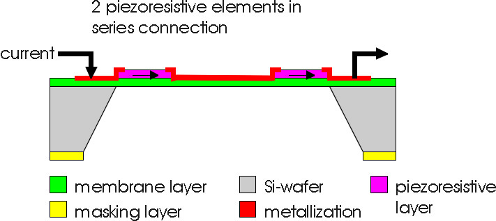 Fig. 5
Piezoelectric Microphones
Design and operation of piezoelectric microphones are comparable to that of piezoresistive microphones (fig. 6). The difference is that materials are used which generate electrical potential differences at their surfaces instead of changing their resistivity. Piezoelectric materials used in silicon microphones are ZnO, PVDF and PZT.
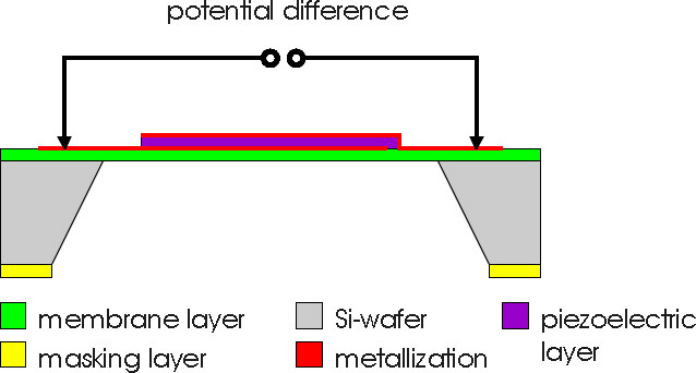 Fig. 6
Optical Microphones
In contrast to the previous transducers, optical microphones modulate light. A sketch can be seen in figure 7 . The microphone consists of two chips. One is the membrane chip and the other is carrying a rigid structure. The membrane together with the structure of the second chip functions as a waveguide. The membrane deflection changes the geometry of the waveguide. This results in a change of intensity and phase of the light signal. Both effects can be detected, the intensity changes directly and the phase changes with an interferometric setup.
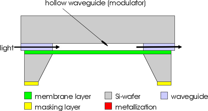 Fig. 7
FET Microphones
The FET microphone is an example of a new principle, which can be realized only by micromechanics. A field effect transistor is modulated indirectly by the acoustical signal.
Figure 8 shows an FET. The field between the metallic gate and the bulk generates a channel through which a current can flow between drain and d Acoustics, Vol 50, No. 1, 1997
Sessler, G.M., Silicon Microphones. In Proc.of 97th Convention of he AES, November 1994. San Francisco, USA