151st ASA Meeting, Providence, RI
Acoustics Says "Nano, Nano" to Materials Characterization
Donna Hurley- hurley@boulder.nist.gov
Malgorzata Kopycinska-Mueller, Tony Kos, Roy Geiss, and Eric Langlois
National Institutes of Science & Technology
325 Broadway
Boulder, CO 80305
Popular version of paper 3aPA2
Presented Wednesday morning, June 7, 2006
151st ASA Meeting, Providence, RI
You know what they say: size matters. Today, the relentless trend is to
smaller and smaller. The emerging field of nanotechnology involves numerous
applications that share a common length scale - from less than a millionth
to a billionth of a meter. Nanotechnology is predicted to generate $340
billion in value of materials and processing within the next 15-20 years.
To realize this potential in applications such as computers, cellphones,
and healthcare, new tools are needed to characterize materials on these
tiny length scales.
Our work focuses on ways to determine nanoscale mechanical properties: how
stiff or compliant a material is (elastic modulus), whether a film or
coating adheres to its substrate, whether a device contains buried defects,
and so on. Information about mechanical properties can be critical to
understanding a device's performance, integrity, or reliability. Moreover,
it is increasingly valuable to visualize how the properties vary throughout
the sample, instead of just using a single "average" number.
Acoustic techniques based on high-frequency vibrations have been invaluable
for materials characterization on larger length scales. Reasons include
their nondestructive nature, visualization or imaging capabilities, and
ability to probe beneath the surface. For nanoscale materials
characterization, we have also chosen an approach based on acoustics. In
this case, our techniques involve an instrument called the atomic force
microscope (AFM). The AFM enables us to probe surfaces on nanometer length
scales by means of a tiny sensor called a cantilever. As shown in Fig. 1,
the AFM cantilever looks like a diving board. It is thinner than a human
hair and contains a nanoscale tip at one end.
Acoustics enters the act when we study how the cantilever beam vibrates.
Using a method called atomic force acoustic microscopy (AFAM), we shake or
vibrate the cantilever when the tip touches a sample. At certain
frequencies, cantilever resonances occur and the vibrational motion is much
stronger. Familiar examples of resonant structures include tuning forks,
bells, and guitar strings. By monitoring the exact frequencies at which the
resonances occur, we can determine the mechanical properties of the sample.
This requires the use of mathematical models that describe the motion of
the cantilever beam and the interaction between the tip and the sample.
AFAM was originally developed to measure properties while the tip remained
motionless at one point on the sample. Recently, we have created tools to
make AFAM measurements while the tip moves across the sample. In this way,
we can obtain nanomechanical maps - quantitative images of nanoscale
properties. Mapping greatly aids our ability to understand samples with
multiple components. Figure 2 shows nanomechanical maps for three different
samples. Images like these show other scientists and engineers how they
might use our tools for their applications. In addition, we are working on
new ways to use these methods to detect other mechanical properties.
Because NIST is the national measurement laboratory for the U.S.,
additional project activities are aimed at improving the accuracy of AFAM
as a measurement technique.
For more detailed technical information, see "Nanoscale elastic-property
measurements and mapping using atomic force acoustic microscopy," D. C.
Hurley, M. Kopycinska-Mueller, A. B. Kos, and R. H. Geiss, Meas. Sci.
Technol. 16, 2167 (2005).
Figures:
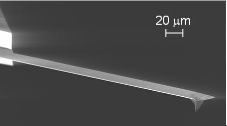
Fig.1. An atomic force microscope (AFM) cantilever sensor. The cantilever
is micromachined from silicon and contains a nanoscale tip (lower right)
that touches the sample of interest. This image was obtained with a
scanning electron microscope.
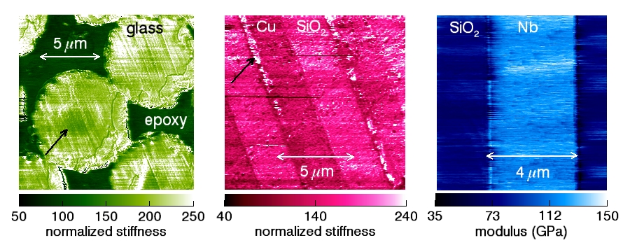
Fig.2. Nanomechanical maps. Each image took less than one hour to create.
The green image corresponds to a sample with glass fibers in epoxy and
shows the relative stiffness of each component. The pink image contains
stripes of copper (Cu) embedded in silica (SiO2). The blue image contains
a thin metal (niobium, Nb) stripe on top of silica and shows the elastic
modulus of each component. All of the images show how AFAM mapping can
distinguish between materials with different mechanical properties
(stiffness and modulus). The black arrows show features that were not
expected: softer areas inside the glass fibers, and a metal (tantalum)
interlayer. These features are virtually invisible in standard AFM maps of
the surface height.
[ Lay Language Paper Index | Press Room ]
|